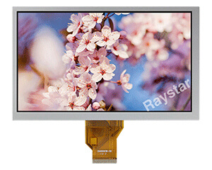
| Item | Dimension | Unit |
|---|---|---|
| TFT Series | IPS TFT LCD,LVDS TFT Display,Wide Temperature TFT,Wide View TFT | |
| Size (Diagonal) | 8.4 | inch |
| Dot Matrix / Resolution | 1024 × 3 (BGR) × 768 | dots |
| Module Dimension | 199.5 × 149.0 × 14.3 | mm |
| Active Area | 170.8032 (H) × 128.1024 (V) | mm |
| Dot / Pixel Pitch | 0.1668 × 0.1668 | mm |
| LCD Type | Normally Black , Transmissive | |
| View Direction | 80/80/80/80 (IPS) | |
| Aspect Ratio | 4:3 | |
| Side screw torque | Typ:0.9 Max:1.3 (Unit,Kgf-cm) | |
| Backlight Type | LED, Normally White | |
| Control Board | No | |
| Power Board | No | |
| TFT Driver IC | ST5821AH+ST5084AA | |
| Interface | LVDS | |
| PCAP FW Version | 00_T1_M03 | |
| PCAP IC | EXC81W32 | |
| PCAP Interface | USB (I2C available) | |
| PCAP Resolution | 16384x16384 | |
| Detect Points | 2 | Points |
| Touch Panel | Projected Capacitive Touch Screen, PCAP | |
| Surface | Glare | |
| Brightness | 400 | cd/㎡ |
| O-Film | No | |
| Mounting Hole | Yes | |
| Operating Temperature | -30~+80 | °C |
| Storage Temperature | -30~+80 | °C |
| Pin No. | Symbol | Function |
|---|---|---|
| 1 | VDD | Power supply |
| 2 | VDD | Power supply |
| 3 | GND | Ground |
| 4 | GND | Ground |
| 5 | Link0- | LVDS differential data input (D0N) |
| 6 | Link0+ | 0+ LVDS differential data input (D0P) |
| 7 | GND | Ground |
| 8 | Link1- | LVDS differential data input (D1N) |
| 9 | Link1+ | 1+ LVDS differential data input (D1P) |
| 10 | GND | Ground |
| 11 | Link2- | 2- LVDS differential data input (D2N) |
| 12 | Link2+ | 2+ LVDS differential data input (D2P) |
| 13 | GND | Ground |
| 14 | CLKIN- | - LVDS differential clock input (CLKN) |
| 15 | CLKIN+ | + LVDS differential clock input (CLKP) |
| 16 | GND | Ground |
| 17 | Link3- | 3- LVDS differential data input (D3N) |
| 18 | Link3+ | 3+ LVDS differential data input (D3P) |
| 19 | MODE | Bit 6/8:Low(6 Bit);High(8 Bit) |
| 20 | SC | Scan direction selector (Low: Normal ;High: Reverse) |
| Pin No. | Symbol | Function |
|---|---|---|
| 1 | NC | No connection |
| 2 | NC | No connection |
| 3 | LED C1 | LED_ Cathode 1 |
| 4 | LED A1 | LED_ Anode 1 |
| 5 | LED A2 | LED_ Anode 2 |
| 6 | LED C2 | LED_ Cathode 2 |
| Pin No. | Symbol | Function |
|---|---|---|
| 1 | USB_VSS | System ground |
| 2 | USB_VDD 5V | Power supply |
| 3 | USB_D+ | Data + |
| 4 | USB_D- | Data - |
| 5 | VSS | System ground |
| 6 | SDA | I2C data input and output (Must be pulled high.) |
| 7 | SCL | I2C clock input (Must be pulled high.) |
| 8 | RST | External Reset, Low is active |
| 9 | INT | External interrupt to the host |
| 10 | VDDT 3.3 | Power supply |

| Item | Symbol | Min | Typ | Max | Unit |
|---|---|---|---|---|---|
| Operating Temperature | TOP | -30 | - | +80 | ℃ |
| Storage Temperature | TST | -30 | - | +80 | ℃ |
| Item | Symbol | Min | Typ | Max | Unit | Remark | |
|---|---|---|---|---|---|---|---|
| Supply Voltage For Logic | VDD | 3.0 | 3.3 | 3.6 | V | ||
| Power Supply For Current | VDD=3.3V | - | 330 | 495 | mA | ||
| Input Voltage | H level | VIH | 0.7VDD | - | VDD | V | SC.MODE |
| L Level | VIL | GND | - | 0.3VDD | V | ||
| Supply PCAP | USB_VDD 5V | 4.4 | 5.0 | 5.5 | V | USB type | |
| I VDD 5V | — | 45 | 68 | mA | |||
| VDDT | 2.8 | 3.3 | 3.5 | V | I2C type | ||
| I VDDT | — | 45 | 68 | mA | |||
| Parameter | Symbol | Min | Typ | Max | Unit |
|---|---|---|---|---|---|
| Supply Voltage of White LED Backlight | VLED | 32.4 | 36 | 40.8 | V |
| Current for LED Backlight | ILED | - | 70*2 | - | mA |
| LED Life Time | - | - | 100,000 | - | Hr |