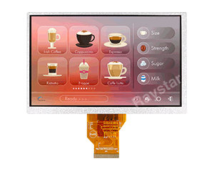
| Item | Dimension | Unit |
|---|---|---|
| TFT Series | IPS TFT LCD,LVDS TFT Display,Wide Temperature TFT,Wide View TFT | |
| Size (Diagonal) | 7 | inch |
| Dot Matrix / Resolution | 800 × RGB × 480 (TFT) | dots |
| Module Dimension | 165.0(W) × 104.6(H) × 5.3(D) | mm |
| Active Area | 152.4 × 91.44 | mm |
| Dot / Pixel Pitch | 0.1905 × 0.1905 | mm |
| LCD Type | TFT, Normally Black, Transmissive | |
| View Direction | 85/85/85/85 (IPS) | |
| Aspect Ratio | 16:9 | |
| Backlight Type | LED, Normally White | |
| Control Board | No | |
| Power Board | No | |
| TFT Driver IC | RM53052+RM57452 | |
| Interface | LVDS | |
| Touch Panel | Without Touch Screen | |
| Surface | Anti-Glare | |
| Brightness | 450 | cd/㎡ |
| O-Film | No | |
| Operating Temperature | -30~+80 | °C |
| Storage Temperature | -30~+80 | °C |
| Pin No. | Symbol | Function |
|---|---|---|
| 1 | VCOM | Common Voltage |
| 2 | VDD | Digital circuit |
| 3 | VDD | Digital circuit |
| 4 | NC | No connection |
| 5 | RESET | Global reset pin |
| 6 | STBYB | Standby mode, Normally pulled high STBYB = “1”, normal operation STBYB = “0”, timing controller, source driver will turn off, all output are High-Z |
| 7 | GND | Ground |
| 8 | RXIN0- | Negative LVDS differential data input |
| 9 | RXIN0+ | Positive LVDS differential data input |
| 10 | GND | Ground |
| 11 | RXIN1- | Negative LVDS differential data input |
| 12 | RXIN1+ | Positive LVDS differential data input |
| 13 | GND | Ground |
| 14 | RXIN2- | Negative LVDS differential data input |
| 15 | RXIN2+ | Positive LVDS differential data input |
| 16 | GND | Ground |
| 17 | RXCLKIN- | Negative LVDS differential clock input |
| 18 | RXCLKIN+ | Positive LVDS differential clock input |
| 19 | GND | Ground |
| 20 | RXIN3- | Negative LVDS differential data input |
| 21 | RXIN3+ | Positive LVDS differential data input |
| 22 | GND | Ground |
| 23 | NC | No connection |
| 24 | NC | No connection |
| 25 | GND | Ground |
| 26 | NC | No connection |
| 27 | NC | No connection |
| 28 | SELB | 6bit/8bit mode select H:8bit / L:6bit |
| 29 | AVDD | Power for Analog Circuit |
| 30 | GND | Ground |
| 31 | NC | No connection |
| 32 | NC | No connection |
| 33 | L/R | Horizontal inversion |
| 34 | U/D | Vertical inversion |
| 35 | VGL | Negative power for TFT |
| 36 | NC | No connection |
| 37 | NC | No connection |
| 38 | VGH | Positive power for TFT |
| 39 | NC | No connection |
| 40 | NC | No connection |
| Pin No. | Symbol | Description |
|---|---|---|
| 1 | VLED+ | Red, LED_ Anode |
| 2 | VLED- | White, LED_ Cathode |

| Item | Symbol | Min | Typ | Max | Unit |
|---|---|---|---|---|---|
| Operating Temperature | TOP | -30 | - | +80 | ℃ |
| Storage Temperature | TST | -30 | - | +80 | ℃ |
| Item | Symbol | Values | Unit | Remark | ||
|---|---|---|---|---|---|---|
| Min. | Typ. | Max. | ||||
| Power Voltage | VDD | 2.9 | 3.3 | 3.6 | V | |
| Analog Power | AVDD | - | 13.0 | - | V | |
| TFT Gate ON Voltage | VGH | - | 25.0 | - | V | |
| TFT Gate OFF Voltage | VGL | - | -5.9 | - | V | |
| TFT Common Voltage | Vcom | - | 6.2 | - | V | |
| Power Current | IDD | - | 19.3 | 29 | mA | VDD=3.3V |
| Analog Power Current | IAVDD | - | 11.5 | 18 | mA | AVDD=13V |
| TFT Gate ON Current | IVGH | - | 0.27 | 1.0 | mA | VGH=25V |
| TFT Gate OFF Current | IVGL | - | 0.27 | 1.0 | mA | VGL=-5.9V |
| TFT Common Current | IVCOM | - | 1.3 | 2 | uA | VCOM=6.2V |
| Parameter | Symbol | Min. | Typ. | Max. | Unit |
|---|---|---|---|---|---|
| LED Current | - | - | 180 | - | mA |
| LED Voltage | VLED+ | 8.4 | 9.0 | 9.6 | V |
| LED Life Time | - | 50,000 | - | - | Hr |